Understanding Impedance Control in PCB Routing: Best Practices and Guidelines
Author : Adrian September 13,solder paste manufacturers 2025Table of Contents
If you're designing a printed circuit board (PCB) for high-speed or high-frequency applications, understanding impedance control in PCB routing is critical. But what exactly is controlled impedance, and how can you implement it effectively? In short, controlled impedance ensures that signals travel through your PCB traces without distortion by maintaining a consistent electrical impedance. This blog will dive deep into the best practices and guidelines for controlled impedance routing, covering key aspects like trace spacing, via placement, and signal return paths to help you achieve optimal signal integrity.
Whether you're an experienced engineer or new to PCB design, this guide will walk you through actionable steps to master impedance control. Let’s explore the details, from fundamental concepts to practical tips, ensuring your designs meet modern performance demands.
What Is Impedance Control in PCB Routing?
Impedance control refers to the process of designing PCB traces to have a specific electrical impedance, which is the measure of opposition to alternating current in a circuit. In high-speed digital and high-frequency analog designs, mismatched impedance can cause signal reflections, crosstalk, and electromagnetic interference (EMI), leading to data errors or system failures. Controlled impedance routing ensures that the impedance of a trace matches the source and load, minimizing these issues.
Impedance is influenced by several factors, including trace width, trace thickness, dielectric material properties, and the distance between the trace and its reference plane (usually a ground or power plane). For example, a typical target impedance for high-speed designs like USB or HDMI interfaces might be 50 ohms for single-ended traces or 100 ohms for differential pairs. Getting this right is crucial for maintaining signal integrity, especially as signal speeds exceed 1 GHz in modern applications.
Why Is Controlled Impedance Important?
In high-speed PCB designs, signals behave more like waves traveling through a transmission line than simple electrical currents. If the impedance along the trace varies, part of the signal wave reflects back, causing distortion. This can result in:
- Signal delays or timing errors.
- Data corruption in digital circuits.
- Increased EMI, affecting nearby traces or components.
For instance, in a DDR4 memory design, impedance mismatches can lead to bit errors, while in RF applications, they can degrade signal power. By following PCB routing guidelines for controlled impedance, you ensure reliable performance, reduced noise, and compliance with industry standards.
Key Factors Affecting Impedance in PCB Design
Before diving into best practices, let’s break down the main factors that influence impedance in PCB routing. Understanding these will help you make informed decisions during design.
1. Trace Width and Thickness
The width and thickness of a trace directly affect its impedance. Wider traces have lower impedance, while narrower traces have higher impedance. For example, a 10-mil-wide trace on a standard 1 oz copper layer might achieve 50 ohms impedance on a specific dielectric material, but adjustments are needed if the material or layer stack changes.
2. Dielectric Material and Thickness
The dielectric constant (Dk) of the PCB substrate material, such as FR-4 (typically Dk = 4.2-4.5), impacts impedance. A lower Dk results in higher impedance for the same trace geometry. The thickness of the dielectric layer between the trace and the reference plane also plays a role—thicker dielectrics increase impedance.
3. Trace Spacing from Reference Planes
The distance between a signal trace and its reference plane (ground or power) affects impedance. Closer proximity to the plane lowers impedance due to increased capacitance. This is why stack-up design is critical for controlled impedance routing.
4. Trace Configuration
Whether a trace is single-ended or part of a differential pair changes the impedance calculation. Differential pairs, often used in high-speed designs like USB or Ethernet, require precise spacing between the two traces to maintain the target differential impedance, such as 90 or 100 ohms.
Best Practices for Controlled Impedance Routing
Now that we understand the basics, let’s explore actionable PCB routing guidelines to achieve controlled impedance. These practices will help you design boards that maintain signal integrity and minimize interference.
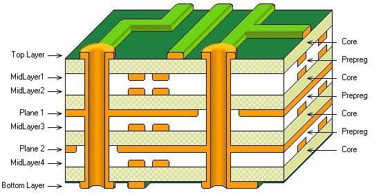
1. Plan Your Stack-Up Early
The PCB stack-up defines the arrangement of signal, ground, and power layers. A well-planned stack-up is the foundation of controlled impedance routing. Ensure that high-speed traces are placed adjacent to a continuous reference plane (usually ground) to provide a consistent return path. For example, in a 4-layer board, place critical signal traces on the top layer with a ground plane directly beneath it.
Work with your PCB manufacturer to select materials with stable dielectric constants and define layer thicknesses that match your impedance targets. Many design tools allow you to simulate impedance based on stack-up parameters before routing begins.
2. Calculate and Set Trace Widths Precisely
Use impedance calculators or simulation software to determine the exact trace width for your target impedance. For instance, achieving a 50-ohm single-ended impedance on a 1.6mm FR-4 board with a 1 oz copper layer might require a trace width of around 10-12 mils, depending on the dielectric thickness. Stick to these calculated widths during routing, and avoid unnecessary variations.
3. Maintain Consistent Trace Spacing
Trace spacing is critical for avoiding crosstalk and maintaining impedance, especially in differential pairs. For differential signals, keep the spacing between the two traces uniform and as per design rules (often 2-3 times the trace width). Also, ensure adequate spacing between unrelated traces to reduce coupling. A common guideline is to maintain a spacing of at least 3 times the trace width (3W rule) between high-speed traces to minimize interference.
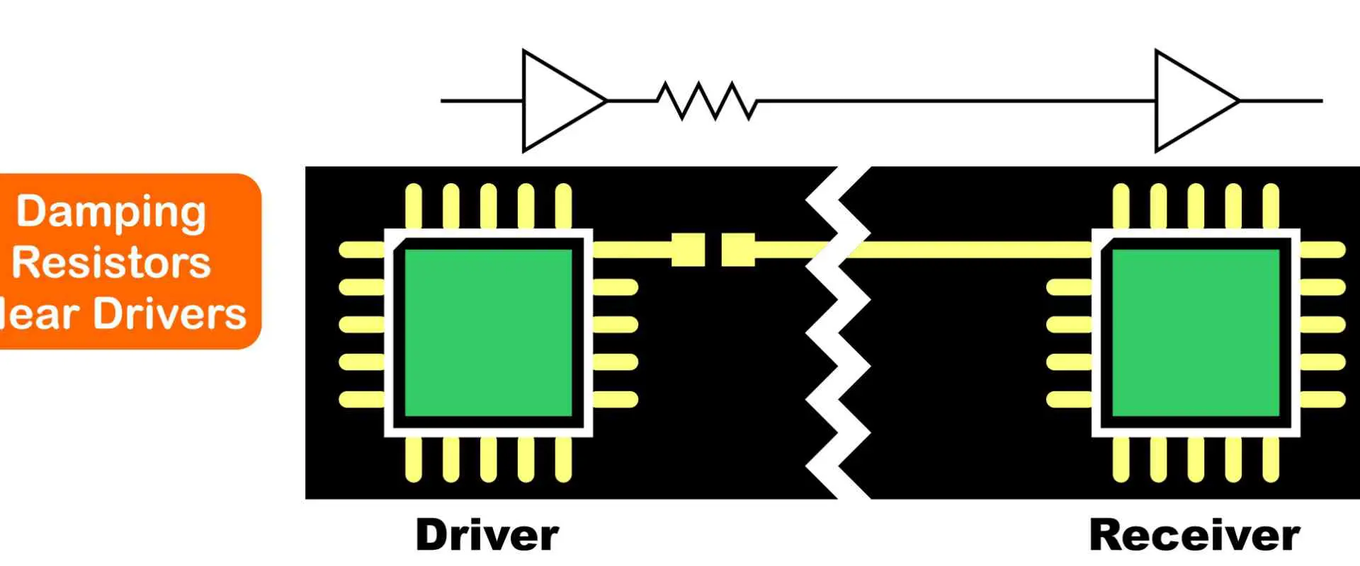
4. Optimize Via Placement for High-Speed Signals
Vias introduce discontinuities in impedance, which can cause signal reflections. To minimize this, follow these via placement guidelines:
- Keep vias to a minimum on high-speed traces. Route signals on a single layer whenever possible.
- Use back-drilling for through-hole vias to remove unused stub lengths, which can act as antennas and cause reflections.
- Place ground vias near signal vias to provide a low-impedance return path. A common practice is to place two ground vias symmetrically around a high-speed signal via.
For example, in a design with a 2.5 GHz signal, a via stub longer than 10 mils can significantly degrade performance. Back-drilling or using blind vias can solve this issue.
5. Ensure a Proper Signal Return Path
A signal return path is the route that the return current takes back to the source, typically through a ground plane. Discontinuities in the return path can increase loop inductance, leading to EMI and signal integrity issues. Follow these tips to ensure a solid return path:
- Avoid splitting ground planes under high-speed traces, as this forces the return current to take a longer, noisier path.
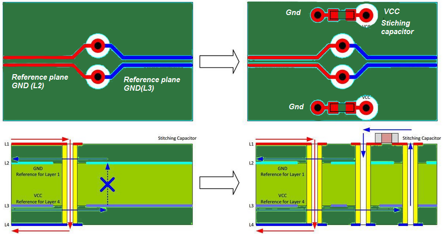
- Route high-speed traces over a continuous reference plane. If a trace must cross a plane split, add stitching capacitors or ground vias to bridge the gap.
- For differential pairs, ensure the return path is balanced to avoid common-mode noise.
6. Route with Minimal Bends and Corners
Sharp corners and abrupt bends in traces can cause impedance discontinuities and signal reflections. When routing high-speed traces, use 45-degree angles or smooth curves instead of 90-degree turns. If a sharp turn is unavoidable, consider using mitered corners to reduce the impact on impedance.
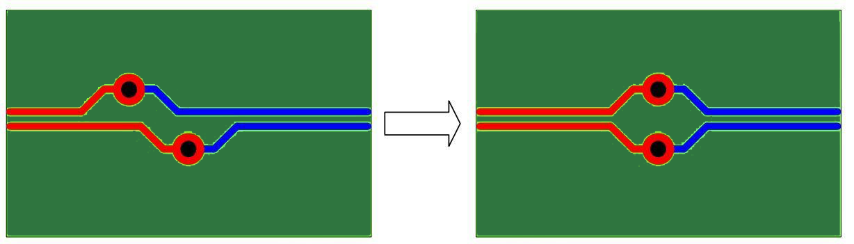
7. Match Trace Lengths for Differential Pairs
In differential signaling, both traces in a pair must have equal lengths to ensure signals arrive at the same time. Length mismatches can cause skew, leading to data errors. Use serpentine routing (adding small loops to a shorter trace) to match lengths, but keep the loops small to avoid adding unnecessary inductance.
Tools and Simulations for Controlled Impedance Design
Modern PCB design software offers built-in tools to help with controlled impedance routing. These tools can calculate trace widths, simulate signal behavior, and highlight potential issues before manufacturing. Some key features to look for include:
- Impedance calculators based on stack-up and material properties.
- Signal integrity analysis to predict reflections and crosstalk.
- Design rule checks (DRC) to enforce trace spacing and width constraints.
Additionally, collaborate with your PCB manufacturer during the design phase. They can provide specific guidelines for their fabrication process, such as tolerances for trace width and dielectric thickness, ensuring your design translates accurately to the final product.
Common Challenges and How to Overcome Them
Even with the best PCB routing guidelines, challenges can arise during controlled impedance design. Here are some common issues and solutions:
1. Manufacturing Variations
Trace widths and dielectric thicknesses can vary slightly during fabrication, affecting impedance. To mitigate this, design with some tolerance (e.g., ±10% of target impedance) and request impedance testing from your manufacturer for critical designs.
2. Mixed Signal Designs
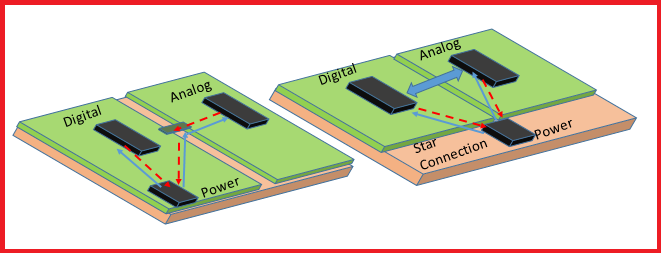
In boards with both analog and digital signals, separating the two domains is essential to avoid interference. Use dedicated ground planes for each domain and route high-speed digital traces away from sensitive analog traces.
3. High-Density Designs
In dense layouts, maintaining trace spacing and via placement rules can be difficult. Prioritize critical signals by routing them first, and use smaller via sizes or microvias to save space without compromising performance.
Final Thoughts on Impedance Control in PCB Routing
Mastering impedance control in PCB routing is essential for high-speed and high-frequency designs. By following the best practices and guidelines outlined in this blog—such as precise trace spacing, strategic via placement, and ensuring a proper signal return path—you can achieve reliable signal integrity and minimize issues like crosstalk and EMI. Start with a well-planned stack-up, use simulation tools to validate your design, and collaborate with your manufacturer to account for fabrication variables.
Implementing controlled impedance routing might seem complex at first, but with attention to detail and adherence to PCB routing guidelines, you’ll create boards that perform consistently under demanding conditions. Keep these tips in mind for your next project, and you’ll be well on your way to designing high-quality, efficient PCBs.

The Role of Flux in PCB Wave Soldering: Selection, Application, and Residue Removal
March 16, 2026PCB wave soldering flux types include rosin, water-soluble, and no-clean options with varying activity levels for oxide removal and solder flow. This guide covers selection criteria, spray foam drop-jet application methods, residue removal processes, and alternatives like nitrogen blanketing to boost joint reliability and yields for engineers.
Article
Achieving Uniform Solder Fillets in PCB Wave Soldering: Process Control
March 16, 2026Achieve uniform solder fillets in PCB wave soldering with process control strategies. Optimize flux, preheat, wave height, conveyor speed for consistent fillet shape, height, and wetting balance. Includes visual inspection tips and troubleshooting for reliable through-hole assemblies. Boost quality in production.
Article
Optimizing Conveyor Speed for Efficient PCB Wave Soldering
March 16, 2026Learn PCB wave soldering conveyor speed calculation to manage dwell time, immersion depth, and throughput effectively. Electric engineers get practical steps, best practices, and troubleshooting tips for higher process efficiency and fewer defects in wave soldering operations.
Article
Understanding IPC Standards for PCB Surface Finishes: Ensuring Quality and Compliance
March 11, 2026Understand IPC standards IPC 4552 ENIG and IPC 4553 immersion silver for PCB surface finishes. Ensure compliance, enhance solderability, and prevent common defects to achieve reliable, high quality circuit boards.
Article
Miniaturization Challenges in PCB Assembly
March 11, 2026Navigate the complexities of high density interconnect PCB assembly and precise component placement. Learn to tackle miniaturization challenges, from tiny part handling to thermal stress, ensuring robust and reliable electronics.
Article
High Speed Routing Techniques: PCB
March 11, 2026Master high speed routing in PCBs to ensure signal integrity and minimize electromagnetic interference. Learn essential techniques for robust designs, from controlled impedance to differential pair strategies. Prevent performance issues and achieve reliable electronics.
ArticleGet Instant PCB
Quotations
Full-featured PCB
manufacturing service at low cost.


 相关文章
相关文章


 精彩导读
精彩导读
 热门资讯
热门资讯 关注我们
关注我们